
Home > Industry Information > Introduction To Switching Power Supply Debugging
This passage introduces switching power supply debugging, a key process for testing and fixing SMPS issues. It covers basic debugging steps, common problems like transformer saturation and startup failure, and a standard troubleshooting procedure. The text emphasizes that systematic debugging is essential for ensuring power supply stability, efficiency, and reliability in modern electronics.
Switching Power Supply Debugging refers to the process of testing, analyzing, and adjusting a switching power supply (SMPS, Switch Mode Power Supply) during design, production, or maintenance in order to identify and resolve faults. A switching power supply converts electrical energy using high-frequency switching devices such as MOSFETs or IGBTs. Because of its high efficiency, small size, and light weight, it is widely used in telecommunications equipment, industrial control systems, computers, electric vehicles, and consumer electronics.
However, the internal structure of a switching power supply is complex. It involves high-frequency switching, electromagnetic interference (EMI), feedback control, and power conversion stages. As a result, various issues may arise during design or operation. Through systematic debugging and fault analysis, engineers can improve the stability, efficiency, and reliability of the power supply.
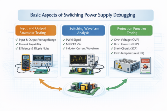
In practical engineering, switching power supply debugging usually involves several key tasks.
The first step in debugging is verifying the basic electrical performance of the power supply, including:
·Input voltage range
·Output voltage stability
·Output current capability
·Efficiency
·Ripple and noise
Engineers typically use instruments such as oscilloscopes, multimeters, and electronic loads to perform these measurements. By analyzing the waveforms and electrical parameters, they can determine whether the power supply is operating correctly.
The core of a switching power supply is high-frequency switching control. Therefore, engineers must observe the waveforms at critical nodes during debugging, such as:
·PWM drive signals
·MOSFET drain-to-source voltage (Vds)
·Inductor current waveform
·Output voltage ripple
These waveforms reflect the operating condition of the power supply, including switching frequency, duty cycle, and switching losses, helping engineers determine whether the circuit is stable.
To ensure safe operation, switching power supplies usually include several protection mechanisms, such as:
·Over-Voltage Protection (OVP)
·Over-Current Protection (OCP)
·Short-Circuit Protection (SCP)
·Over-Temperature Protection (OTP)
During debugging, abnormal conditions are simulated to verify that these protection circuits are triggered properly.
During the debugging process, engineers often encounter several typical problems.
Transformer saturation occurs when the magnetic flux density of the transformer core exceeds its limit. When this happens, the inductance collapses and the current increases rapidly, which may damage switching devices such as MOSFETs.
Common causes include:
·Improper transformer turn design
·Excessive current limit settings
·Large inrush current during startup
Typical solutions include optimizing the transformer design or adding a soft-start circuit.
If the drain-to-source voltage (Vds) of the MOSFET exceeds its rated limit, the device may fail.
Possible causes include:
·Voltage spikes caused by leakage inductance
·Excessive reflected voltage from the transformer
·Improper snubber circuit design
·Common solutions include:
·Adding RCD or TVS snubber circuits
·Optimizing transformer winding design
·Reducing leakage inductance
Excessive temperature in the control IC may occur due to several factors:
·High switching losses
·Poor PCB heat dissipation
·High ambient temperature
This problem can be mitigated by increasing copper area for heat dissipation, improving PCB layout, or reducing switching losses.
Some switching power supplies may fail to start when there is no load or only a light load. In such cases, the power supply may repeatedly start and shut down.
·Common reasons include:
·Insufficient voltage from the auxiliary winding supplying Vcc
·Improper startup resistor design
Possible solutions include increasing the number of turns in the auxiliary winding or adding a dummy load.
Under light-load or no-load conditions, the output voltage may show significant ripple, affecting power stability.
Possible causes include:
·The controller entering burst mode
·Insufficient output capacitance
The issue can often be resolved by increasing the output capacitor or optimizing the control parameters.

In engineering practice, debugging usually follows these steps.
Static Inspection
·Check PCB soldering quality
·Verify component models and polarity
·Check for short circuits or open circuits
Low-Voltage Startup Test
The circuit should first be powered with a low voltage or an isolated power source to prevent component damage caused by high voltage.
Waveform Measurement
Use an oscilloscope to observe key signals, such as:
·PWM signals
·MOSFET gate drive waveforms
·Inductor current waveforms
Load Testing
Gradually increase the load while monitoring:
·Output voltage stability
·Temperature rise
·Efficiency performance
Stress and Limit Testing
This includes:
·Short-circuit testing
·Overload testing
·High-temperature testing

Switching power supply debugging plays a critical role in electronic product development.
Improves system stability
Reduces failure rates
Enhances power efficiency
Ensures compliance with safety standards
In modern electronic systems, switching power supplies serve as the core power module of most devices. Therefore, a thorough debugging process is essential to ensure stable, efficient, and safe operation.
Switching Power Supply Debugging is an essential step in the design, development, and maintenance of power electronics. By systematically testing waveforms, electrical parameters, and protection functions, engineers can identify common issues such as transformer saturation, MOSFET over-voltage stress, startup failure, and excessive output ripple. Through proper circuit optimization and parameter adjustment, these problems can be resolved, ensuring reliable and efficient power supply performance.
Industry Information