
Home > Industry Information > What Is QFP Package: Features, Types, And Application Fields
This passage provides a comprehensive analysis of Quad Flat Package (QFP) technology. It covers the basic structure and technical features of QFP, including its four-sided gull-wing leads, various pitch options, and material types. The document details different QFP classifications based on thickness and pitch, along with various improved types. It explores QFP's wide application fields, manufacturing processes, and compares it with other packaging technologies like BGA and QFN. Finally, it discusses the current status and development trends of QFP packaging.
Quad Flat Package (QFP) is a surface-mount integrated circuit packaging form with gull-wing leads extending from all four sides. This packaging technology features leads with pitches as low as 0.3mm and a maximum lead count of up to 304.
QFP packaging is used not only for digital logic LSI circuits such as microprocessors and gate arrays but also for analog LSI circuits like VTR signal processing and audio signal processing. Its widespread adoption has made it an indispensable packaging technology in modern electronic devices.
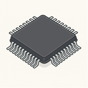
QFP packaging employs a four-sided lead design, with leads extending from all four sides in a gull-wing (L) shape. This structure allows QFP packaging to accommodate a large number of leads within a limited space, meeting the requirements of complex integrated circuits.
The packaging substrates mainly include three types: ceramic, metal, and plastic. Plastic packaging constitutes the vast majority in terms of quantity, which is why when no specific material is indicated, it usually refers to plastic QFP.
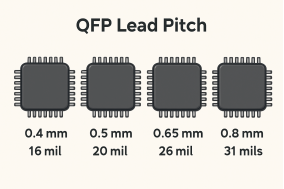
Lead pitch specifications vary, including 1.0mm, 0.8mm, 0.65mm, 0.5mm, 0.4mm, and 0.3mm, among others. These different lead spacings enable QFP packaging to adapt to chips with varying integration levels, offering extremely high flexibility.
QFP packaging is suitable for PCB mounting and routing using SMT surface mount technology. This characteristic gives it a natural advantage in modern electronic manufacturing, as SMT technology enables high-density, high-efficiency circuit board assembly.
QFP packaging has low parasitic parameters, making it suitable for high-frequency applications. This feature allows it to perform excellently in high-frequency circuits, meeting the needs of communication and other fields.
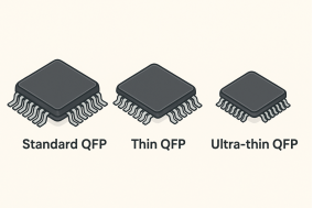
Based on package body thickness, QFP packaging can be categorized into standard, thin, and ultra-thin types.
Standard QFP thickness ranges between 2.0-3.6mm, thin LQFP thickness is 1.4mm, and ultra-thin TQFP thickness is only 1.0mm. This classification, established by the Japan Electronics and Mechanical Industries Association, primarily addresses the trend toward thinner and lighter electronic products.
Classified by lead pitch, QFP has regular pitch and fine pitch variations.
QFPs with lead center distances less than 0.65mm are often called Fine Pitch QFP (FQFP). As lead pitch decreases, the issue of lead bending becomes more prominent, requiring more precise soldering processes.
To overcome the limitations of traditional QFP, various improved QFP packaging types have been developed:
BQFP with cushion pads: Features resin cushion pads at the four corners of the package to prevent lead bending during transportation and installation.
GQFP with guard ring: Uses a resin guard ring to cover the lead tips, providing better protection.
Heat-enhanced HQFP: Improves thermal performance through enhanced package structure or materials, suitable for high-power chips.
QFP with heat spreader: Such as the HS-QFP introduced by ASE, using embedded heat spreader design to increase power handling capacity by 50%.
Exposed pad L(T)QFP: Directly connects to the PCB through an exposed pad, significantly improving thermal performance, with thermal resistance only half that of standard packaging.
QFP packaging is widely used in microprocessors and digital logic circuits.
Its multi-lead characteristics enable it to meet the interface requirements of complex processors, making it a popular multi-lead LSI packaging solution.
In the automotive electronics field, QFP packaging also holds an important position. Automotive electronic control systems have extremely high requirements for reliability and space utilization. QFP packaging meets these needs, especially products compliant with automotive electronic grade certifications such as AEC-Q100 Grade 0.
Communication equipment is another important application area for QFP packaging. Signal processing chips in communication equipment often use QFP packaging, particularly in high-frequency application scenarios where QFP's low parasitic parameter advantages are fully utilized.
Portable consumer electronic products, such as PDAs, digital cameras, and mobile phones, also widely use QFP packaging.These products have strict requirements for component size and power consumption, which thin LQFP and ultra-thin TQFP precisely meet.
In industrial control systems, QFP packaging continues to play a role in components such as power controllers and microcontrollers due to its good reliability and performance.Industrial environments impose high demands on component stability and temperature adaptability, which QFP packaging can meet under these harsh conditions.

The manufacturing process of QFP packaging involves multiple steps including solder paste printing, component placement, reflow soldering, and X-ray inspection.
Precise control of these process steps is crucial for ensuring packaging quality, with required yield rates exceeding 99.5%.
In terms of soldering, QFP packaging primarily uses SMT surface mount technology.
This technology doesn't require drilling holes in the main board, only aligning the chip leads with corresponding board pads and achieving connection through reflow soldering.
For QFP packaging repair and rework, there are professional operation methods.
These include techniques such as using solder wick to remove solder and fine wire to assist in chip removal. These methods require skilled operators to perform to avoid further damage to the leads.
QFP packaging, especially types with small lead pitch, has extremely high requirements for soldering processes.
Lead coplanarity (all leads on the same plane) is a key factor in ensuring good soldering, as any deviation may lead to soldering failure.
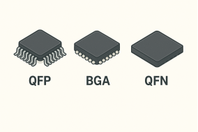
Compared with BGA (Ball Grid Array) packaging, QFP has advantages of easy repair and visual inspection.
BGA packaging joints are invisible after soldering, requiring specialized equipment like infrared for inspection, while QFP lead soldering conditions can be directly visually inspected.
However, BGA has advantages in high pin count and fine pitch aspects.
BGA can achieve required electrical performance through changes in chip substrate structure, offering much greater structural freedom than QFP.
Compared with QFN (Quad Flat No-lead) packaging, QFN is based on lead frame technology, using semi-packaging technology with exposed chip solder pads and tiny finger areas that connect the chip, bond wires, and PCB.
QFN packaging is suitable for applications operating above 12GHz and provides enhanced thermal and electrical performance.
Compared with PGA (Pin Grid Array) packaging, PGA features pin arrays arranged in square matrices on the chip bottom, which can form 2-5 circles depending on pin count, requiring specialized PGA sockets for installation.
QFP, in contrast, is directly soldered onto the PCB surface without additional sockets.
Although QFP packaging has been replaced by TSOP-II and BGA packaging in fields like memory, it still maintains importance in automotive electronics, communication equipment, and industrial control fields.Its mature technology and relatively low cost keep it competitive in these areas.
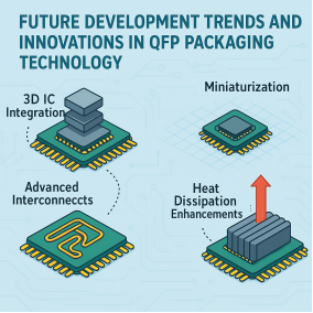
As electronic products develop toward lighter, thinner, shorter, and smaller directions, demand for thin LQFP and ultra-thin TQFP continues to grow.
These thin packages are particularly suitable for portable consumer electronic products like smartphones and tablets that have strict thickness requirements.
To adapt to higher-performance applications, QFP packaging is also innovating in thermal technology.In the future, QFP packaging may integrate with System-in-Package (SiP) technology, achieving higher integration levels and more functions through multi-chip module/stacked structure designs while maintaining traditional QFP form factors.
With technological advancements, QFP packaging continues to evolve. QFP with embedded heat spreaders can increase power handling capacity by 50%, and exposed pad designs reduce thermal resistance by half. These innovations allow QFP packaging to maintain competitiveness in high-performance, high heat dissipation demand scenarios.
Looking forward, QFP packaging might gradually be replaced by advanced packaging like BGA and CSP in specific fields, but its mature processes, low cost, and sufficient performance ensure its irreplaceability in mid-range applications.
In summary, QFP remains a vital IC packaging solution despite competition from newer technologies. Its four-sided gull-wing design offers an excellent balance of pin count, SMT compatibility, and inspection ease. While being replaced by BGA and CSP in high-performance applications, QFP maintains strong positions in automotive, industrial, and consumer electronics. Its mature manufacturing process, cost-effectiveness, and continuous thermal improvements ensure QFP's ongoing relevance in mid-range applications, securing its place in the electronics industry for the foreseeable future.
Industry Information